
|
Magic Mailing List |
|
From: Stefanos Sidiropoulos (stefanos AT rambus DOT com) Date: Wed Apr 05 2000 - 17:58:57 EDT
> maybe i've misunderstood you.  what i'm talking about is that, if you

You indeed misunderstand me...


> look at the attached .mag file with a non-silicided process techfile,
> like SCNA.80.tech27, the wells labelled 'pw' and 'nw' will *not* be
> connected to gnd and vdd, respectively, since there will be n+/p+
> junctions between the transistor diffusions and the ohmic diffusions
> (well-contacts).  however, if you use a silicided process techfile,
> like SCN3M_SUBM.30.tech27, you will see that the wells are connected
> to their respective supplies, since the silicide removes those n+/p+
> junctions, reflecting the fabricated part.  it may be a "weak"
> connection but it doesn't have to carry much current (hopefully) to
> keep the wells biased.  however, how can i make this clearer, it's NOT
> weak!
>

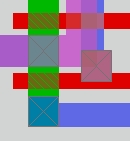
Now take a look on the attached magic file (which is the same as yours
with just a slight change). I am not saying that a designer would do that
willingly but the point of extraction/LVS/simulation is to catch
such mistakes. However, your SCN3M_SUBM.30.tech27 will happilly say
that the source of the PMOS is connected nicely to vdd. You can argue
that this particular cell might work but a similar connection can carry
a LOT of current and definitely is VERY WEAK. Hope that is clear now.

-- Stefanos

magic
tech scmos
timestamp 954970860
<< pwell >>
rect 3 0 19 24
<< nwell >>
rect 3 24 19 48
<< polysilicon >>
rect 4 34 9 36
rect 13 34 15 36
rect 4 26 6 34
rect 4 14 6 22
rect 4 12 9 14
rect 13 12 15 14
<< ndiffusion >>
rect 9 14 13 15
rect 9 11 13 12
<< pdiffusion >>
rect 9 36 13 41
rect 9 33 13 34
<< metal1 >>
rect 0 41 9 45
rect 13 41 19 45
rect 9 26 13 29
rect 9 22 17 26
rect 9 19 13 22
rect 0 7 9 11
rect 13 7 19 11
rect 0 3 19 7
<< ntransistor >>
rect 9 12 13 14
<< ptransistor >>
rect 9 34 13 36
<< polycontact >>
rect 2 22 6 26
<< ndcontact >>
rect 9 15 13 19
rect 9 7 13 11
<< pdcontact >>
rect 9 29 13 33
<< nsubstratencontact >>
rect 9 41 13 45
<< psubstratepdiff >>
rect 9 3 13 7
<< labels >>
rlabel metal1 6 7 6 7 2 gnd:1
rlabel metal1 6 41 6 41 4 vdd:1
rlabel pwell 17 18 17 18 7 pw
rlabel nwell 17 29 17 29 7 nw
<< end >>
|
|
|

|